Preview →
Graphene news (June’s update)
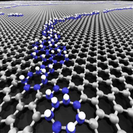
Research on graphene-based materials seems to be getting to a new level of activity. Indeed, we have witnessed an impressive set of experiments since our last update in March. This time one of the magic words is ‘control’. Electrical control of the stacking between layers in trilayer graphene [1]; optical control in the case of the photo-induced doping achieved in Ref. [2]; control of graphene plasmons [3] and of the interaction with a substrate [4]. One should also mention a few of the best available images of defects in graphene (line-defects [5] and vacancies in ion irradiated samples [6]) and the puzzling observation of length-dependent thermal conductivity [7]. We would also like to mention a review on a hot topic: Transport and Grain Boundaries in Poly-crystalline Graphene [8].
[1] “Electric field control of soliton motion and stacking in trilayer graphene”,
M. Yankowitz, J.l I-Jan Wang, A. Glen Birdwell, Yu-An Chen, K. Watanabe, T. Taniguchi, P. Jacquod, P. San-Jose, P. Jarillo-Herrero & B. J. LeRoy, Nature Materials (2014), doi:10.1038/nmat3965
[2] “Photoinduced doping in heterostructures of graphene and boron nitride”,
L. Ju, J. Velasco Jr, E. Huang, S. Kahn, C. Nosiglia, Hsin-Zon Tsai, W. Yang, T. Taniguchi, K. Watanabe, Y. Zhang, G. Zhang, M. Crommie, A. Zettl & F. Wang, Nature Nanotechnology 9, 348–352 [3] “Controlling graphene plasmons with resonant metal antennas and spatial conductivity patterns”,
P. Alonso-González, A. Y. Nikitin, F. Golmar, A. Centeno, A. Pesquera, S. Vélez, J. Chen, G. Navickaite, F. Koppens, A. Zurutuza, F. Casanova, L. E. Hueso, and R. Hillenbrand, Science (2014) DOI: 10.1126/science.1253202
[4] “Commensurate–incommensurate transition in graphene on hexagonal boron nitride”,
C. R. Woods, L. Britnell, A. Eckmann, R. S. Ma, J. C. Lu, H. M. Guo, X. Lin, G. L. Yu, Y. Cao, R. V. Gorbachev, A. V. Kretinin, J. Park, L. A. Ponomarenko, M. I. Katsnelson, Yu. N. Gornostyrev, K. Watanabe, T. Taniguchi, C. Casiraghi, H-J. Gao, A. K. Geim & K. S. Novoselov, Nature Physics 10, 451–456 (2014).
[5] “Controlled growth of a line defect in graphene and implications for gate-tunable valley filtering”,
J.-H. Chen, G. Autès, N. Alem, F. Gargiulo, A. Gautam, M. Linck, C. Kisielowski, O. V. Yazyev, S. G. Louie, A. Zettl, Phys. Rev. B 89, 121407(R) (2014).
[6] “Non-invasive transmission electron microscopy of vacancy defects in graphene produced by ion irradiation”,
Ossi Lehtinen, I-Ling Tsai, Rashid Jalil, Rahul R. Nair, Juhani Keinonen, Ute Kaiser, Irina V. Grigorieva, Nanoscale 6, 6569-6576 (2014).
[7] “Length-dependent thermal conductivity in suspended single-layer graphene”,
Xiangfan Xu, Luiz F. C. Pereira, Yu Wang, Jing Wu, Kaiwen Zhang, Xiangming Zhao, Sukang Bae, Cong Tinh Bui, Rongguo Xie, John T. L. Thong, Byung Hee Hong, Kian Ping Loh, Davide Donadio, Baowen Li & Barbaros Özyilmaz, Nature Communications 5, 3689 (2014).
[8] “Charge Transport in Polycrystalline Graphene: Challenges and Opportunities”.
Aron W. Cummings, Dinh Loc Duong, Van Luan Nguyen, Dinh Van Tuan, Jani Kotakoski, Jose Eduardo Barrios Vargas, Young Hee Lee,* and Stephan Roche, Advanced Materials 2014, DOI: 10.1002/adma.201401389


